
Electrostatic Discharge (ESD) is a physical phenomenon that our electronic devices often experience nearly every day. For engineers working in the electronics industry, ESD is a critical topic as it is known to cause product failures due to failures in sensitive electronics, network downtime and production losses that total US$ 25B per year!
ESD is a sudden and momentary electric current that flows between two objects at different electrical potentials. This increase of static electricity can happen through friction or electrostatic induction. The discharge occurs when two differently charged objects are brought together, or if micro cracks develop in the PCB dielectric substrate. Sometimes ESD can result in a visible spark, which will be generated if the electric field strength is above 4kV/cm.
An EMC compliant product undergoes ESD related safety measures during manufacturing and transport but the most important step to prevent failures through ESD is to properly assess these effects as early as possible during your product design phase.
An ESD Test is generally conducted using a human body model (HBM) and a specific circuit to test the sensitivity of electronic devices. A capacitance of 100pF is charged with a high voltage and discharged via a load resistance of 1,500 Ohm connected at the ends of the Device under Test (DUT). An ESD gun provides a high voltage pulse to put your device under test.
The tests are maintained by standards with common procedures defined in JEDEC 22-A114-B-standards, MIL-STD-883-methodology 3015 and ESD STM5.1 of the ESD association. The specification IEC/EN 61000-4-2 is used to align with norms of the European Union specifically for devices in information technology.
Failures are categorized into two groups: a catastrophic failure is a functional failure which can easily be observed. The 2nd category is an upset failure which can remain undetected. This latter test can be very costly to manufacturers as often the devices are shipped to customers before the issue comes to light – resulting in many product failures and costly recalls or warranty claims.
For manufacturers still using a purely physical prototyping approach, it is necessary to invest in the building of at least one prototype before a laboratory ESD test can be undertaken. If your product then fails this ESD test, there is a cascading effect which extends your product design cycle and increases all associated costs (due to re-designs, building of another prototype, and conducting another series of physical tests).
How does Virtual ESD Testing boost product reliability & decrease EMC costs?
In this blog, we offer a brief overview of how to conduct a virtual test once your PCB design is completed in your ECAD software, such as Altium.
ESD Virtual Tests using computer simulations usually consist of three parts. Part I is a circuit model that contains a representation of your ESD gun: a charge/discharge model and, if required, the human body. A pulse is applied to the circuit just like it is done in a practical test. The circuit also contains the load and can capture measures you want to undertake to reduce the impact of ESD.
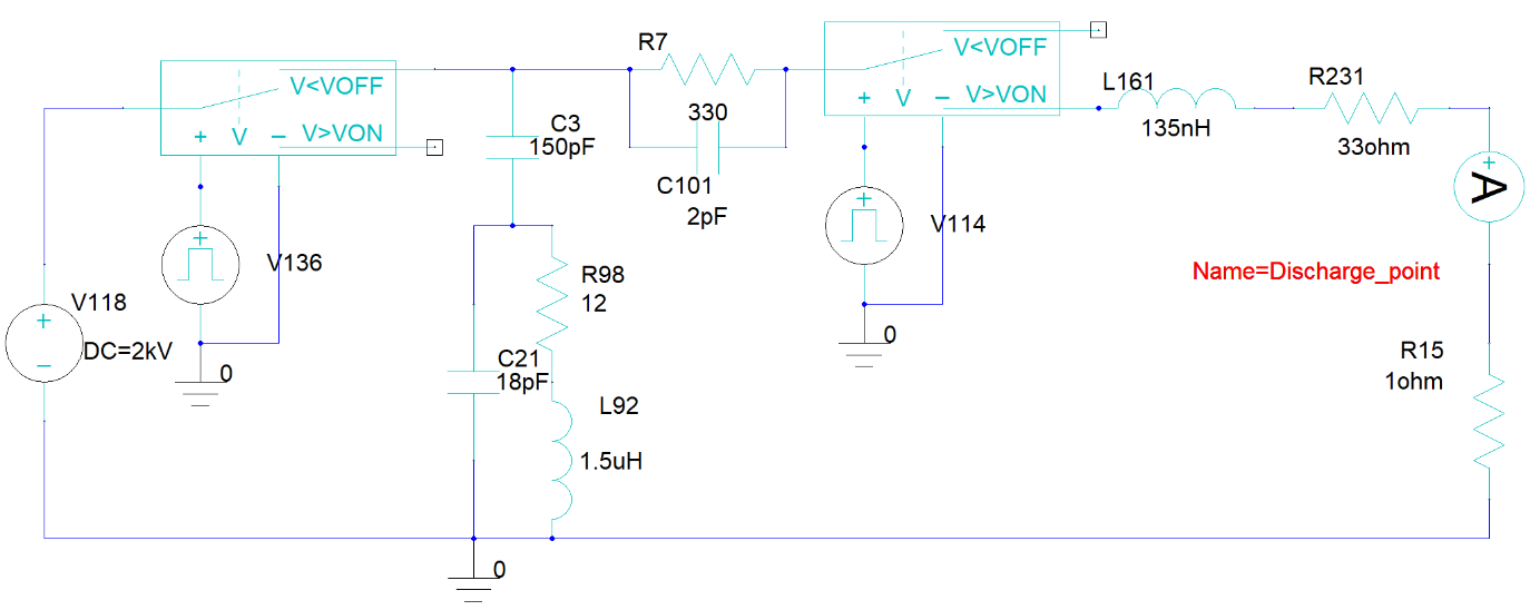
Fig.1: Two Switches operate in alternate conditions. If the Charge Model on the left-hand side is on, the right-hand side switch representing the discharge model is off. ESD counter measures such as diodes, beads or varistors can be tested in this circuit as well. A simulation model like this provides a superb reproducibility and solves fast.
In Part II this model is extended by including the detailed representation of the device you wish to test. This can be a 3D structure or a PCB (or a mix of both) to model full electronic units and the complete product. In Ansys, a very efficient model can be created by merging ECAD and MCAD data within the same environment – an example can be seen in Fig.2 below. In this case, the circuit seen in Fig.1 has been connected to the 3D model.
Beads are applied very close to the AC-DC adaptor and used to avoid any impacting noises (or discharge noise). Additionally, a varistor has been used at the AC-DC adaptor connector in order to make the short circuit between the DC+ and DC Ground when large ESD noise comes in. Results can be visualized as a current distribution on the board and easily be compared. The engineer is also able to measure induced voltages in nearby traces and set current probes and visualize the electric Field Strength E anywhere within the model.
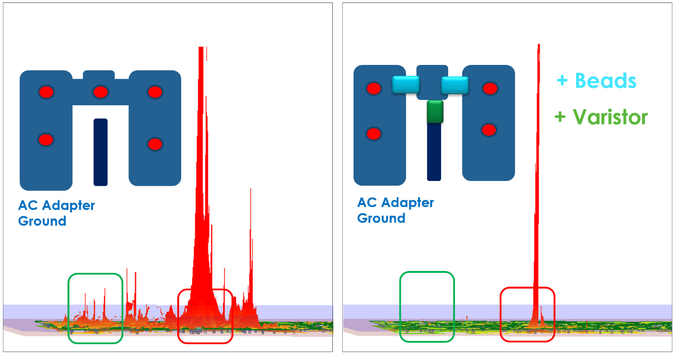
Fig.2: example: current distribution around IC terminals in a 2.5D PCB simulation before (left-hand side) and after (right-hand-side) modifying the Board (1kV@100MHz), The difference can easily be observed and effects studied.
“What about situations were contact discharge is not feasible?”
IEC 61000-4-2 states “Contact discharge is the preferred test method. Air discharges shall be used where contact discharge cannot be applied.” This method is included in our simulation model in Part III of our virtual testing process. To create an accurate model, we require the ECAD data and material composition, and we intend to accurately recreate the current waveform that is generated during the arc formation from an ESD Gun.
Our simulation in Ansys solves the electric potential and Electric Field Strength E in the model and determines the probability of breakdown in each element. During an arc, each element that undergoes breakdown has its conductivity changed to 𝜎𝐼𝑛𝑡𝑟𝑎. Once the arc event finishes, all arc elements have their conductivity changed to 𝜎𝑃𝑜𝑠𝑡. In addition, non-linear chemistry for arcing in air is leveraged from ANSYS EMA3D knowledge of corona formation.

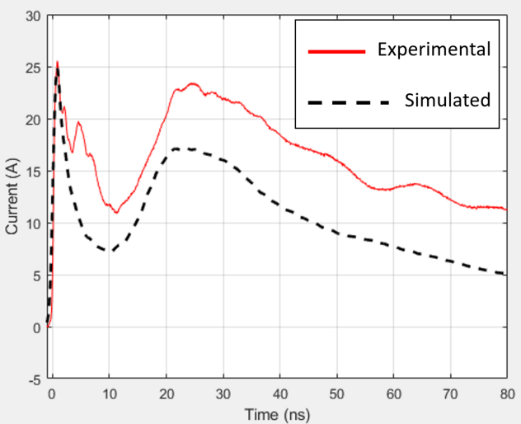
Fig.3: Example showing current waveform reproduced according to IEC 61000-4-4 with Ansys EMA3D recreating the exact waveform generated by an ESD Gun
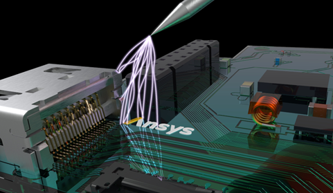
As a practical example we can simulate a discharge test over air on a printed circuit board including several connectors and a specific shape of a discharge tip, as shown in Fig 4 below.
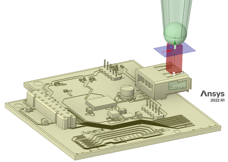
Fig.4: Air discharge ESD test on a PCB. The tip is explicitly modelled and positioned at a specific distance to the connector. The red box represents the domain where the full-wave electromagnetics are combined with non-linear air chemistry and the previously described procedure of conductivity changes.
In the animation shown in Fig. 5 below, visualisation of the Electric Field Strength (E) shows how the arc is formed, which can be easily simulated to understand the effect of variables such as:
- position and shape of the tip,
- component shapes, materials and location on PCB,
- environmental conditions such as air temperature and pressure.
As this is a transient simulation the entire arc forming process can be studied: from its build up stage to the arcing itself with resulting induced voltages in nearby traces and emissions.

Fig.5: Electric Field Strength E to visualise arc formation
What’s next?
We hope you’ve seen just how useful Ansys simulation can be when running virtual ESD tests. Engineers can use their existing ECAD and MCAD data and quickly perform tests using the correct pulse profiles from standard tests such as JEDEC 22-A114-B-standards or MIL-STD-883-methodology 3015. Accurate ESD results for both contact and air discharges are possible by accounting for the presence of fluid conservation equations and an accurate representation of the generation of charge carriers, combined with full-wave electromagnetic effects.
The method we’ve described can be applied directly after a PCB has been designed in CAD (but before a physical prototype is built) to help identify ESD design risks early, as well as assessing various solutions such as grounding strategies and circuit components (such as beads, varistors and diodes). To get started with ESD Simulations in Ansys, click here to start talking with LEAP’s electromagnetics team.