With the trend of more densely packed integrated circuits (ICs) & increased layers in printed circuit boards (PCBs), thermal design becomes critical to the success of new electronic products. We all know intuitively that excessive heat is the enemy of electronic parts, and many engineers work to the rule of thumb that a 10-degree higher temperature rise will lead to a halving in product life expectancy. To push the envelope in PCB design, engineers are using DCIR combined with thermal analysis to push for increased PCB reliability and quality.
“A 10-degree higher temperature rise will lead to half life expectancy”
IR-drop describes the DC voltage that develops across a conductor as a result of its electrical resistance. This voltage is proportional to the current that flows through the conductor and results in a decrease in voltage available at the load devices. For a given power plane, a larger current will result in a greater IR-drop voltage, and hence a lower voltage available at the load. Such voltage drops can cause major problems when distributing power across a PCB; when the drop becomes excessive the voltage at the load may fail to meet necessary device specifications.
The ANSYS SIwave is a tool suitable for such design applications. It is made for PCB designers and EMC specialists alike and provides proven workflows for your PCB design.
Fast configuration DC IR Drop Analysis
The ANSYS SIwave is a dedicated tool that allows users to import electrical CAD (ECAD) data to predict electrical behaviour and performance from all major ECAD packages like Cadence, Zuken, and of course the most common for our Australian customers: Altium Designer.
“Is my voltage regulator supplying the proper DC voltage to all active components attached to the power rails?”
To make the analysis as easy as possible for PCB designers SIwave offers a DC IR Drop Analysis Wizard. Simply select the nets to be investigated and devices connected to those nets will be displayed instantly. That enables easy assignment of current sinks and voltage sources operated on those nets. After a validation check, we can launch DCIR Analysis, compute DC current and voltage distribution across the board and ICs.
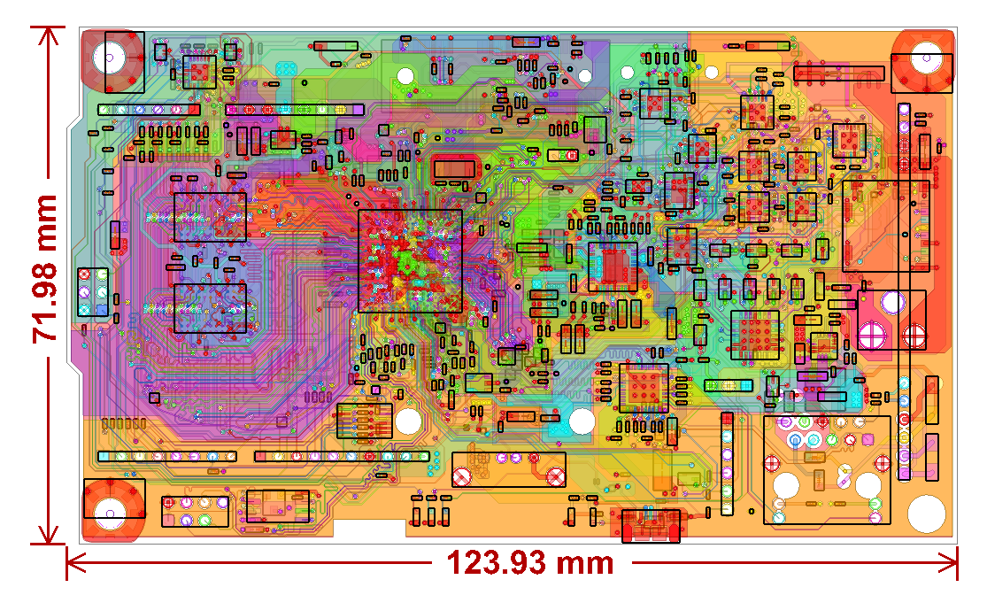
Figure 2 – PCB to be investigated: The model consists of RLC lumped components, pad stacks, vias, traces and the 6-layer structure. Nets are colour coded.
DC Simulation Results
We have now setup and run a DCIR analysis in ANSYS SIwave. The Software employs an automatic adaptive mesh refinement process which produces a mesh that delivers most accurate results within the shortest possible simulation time. No additional user input is needed.
“Adaptive automated meshing for DC Analysis is a key benefit as it minimizes the setup efforts and increases output accuracy at the same time”
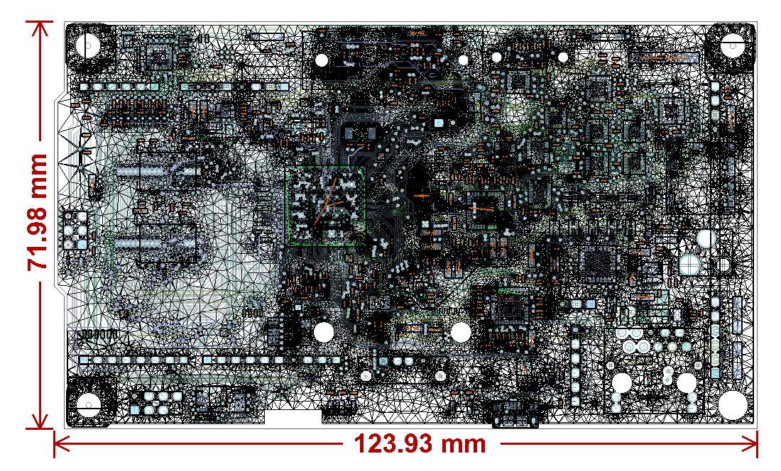
Figure 3 – Final mesh of the PCB after adaptive refinement. Areas with high gradients are meshed with a finer tetrahedral grid.
Let us have a look at the results. The SIwave DC solver computes the DC voltage drop and current density for the entire board. It also calculates the I2R-drop and current flow within all conductive parts of your PCB like vias and traces. The current density plot and the final mesh for the PCB are shown in Figures 3 and 4. In addition, ANSYS SIwave automatically generates a simulation report on voltage and current.
It is the purpose of the power distribution network (PDN) to distribute a stable low noise DC voltage to the active devices on the board.
The user can specify a voltage range for a given power plane and let SIwave automatically point the user to those nets that fails the requirement. Further improvements can be made by modifying layout and changing components.
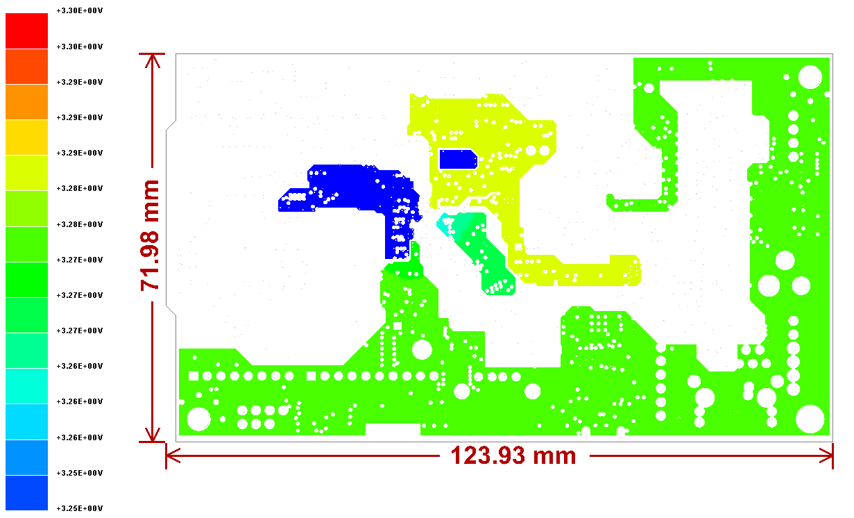
Figure 4 – Voltage plot gives the engineer a feedback on the voltage distribution of the power planes, indicating how much the local voltage drop is from the power plane rated voltage, and whether it is acceptable.
To keep the voltage stable DC resistivity has to be minimized. That can be done by widen the power nets and/or by avoiding any discontinuities. But how to quantify performance of a power net?
SIwave offers a DC path Resistance solver that provides lumped path resistance between points on a plane or trace.
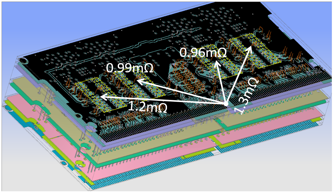
Figure 5 – DC Path Resistance solver gives the engineer a matrix of path resistance from power sources to chips. The lower the path resistance, the better the circuit design is.
Current crowding is another potential challenge SIwave lets you look at and resolve.
The Current density plot gives you an accurate estimation of the current density anywhere on your PDM. That helps you to identify and resolve localized overheating and potential damage to the PCB later in the field
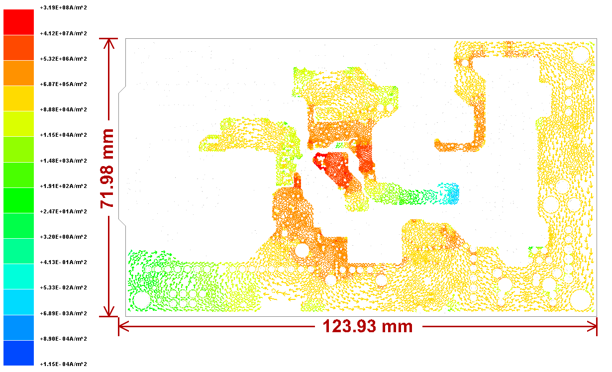
Figure 6 – Current Density plot gives the engineer a feedback on the location of current crowding and bottle necks. Very high current densities can lead to safety risk and high temperature rise. Widening traces can solve potential issues.
For more specific results on that topic of localised overheating the power density can give an indication of potential areas of overheating as well.
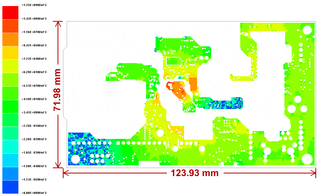
Figure 7 – Power Density plot gives the engineer a feedback on the location of power crowding. Very high power densities can lead to high temperature rise. Widening traces and adding heatsinks can solve potential issues. Identifying those locations is the first step of resolving them before a physical prototype is build.
With the presented workflow a DCIR analysis can be run within minutes after the layout of the PCB has been created. It is the perfect analysis to accompany the design process and gives the engineer a fast feedback on potential issues in the PDN directly after the drafting process.
Co-Simulation with ANSYS IcePak for Temperature Rise
After the DCIR analysis has been performed in SIwave, IcePak will use the imported power maps for the board to perform a thermal analysis. All conductor losses from SIwave across the board serve as the input for the thermal analysis.
IcePak is an App for Electronics Cooling based on the advanced ANSYS Fluent technology. It provides easy to use components like fans, heat sinks, chip models and more to electrical engineers who want to perform high end thermal calculations. It is highly integrated into the ANSYS Electronics Tools. The PCB design and setup information are transferred automatically to IcePak together with the DC power loss maps from the SIwave analysis. All conductors behave temperature dependent.
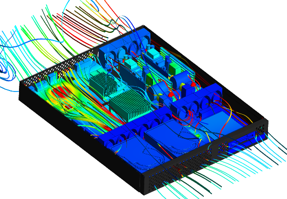
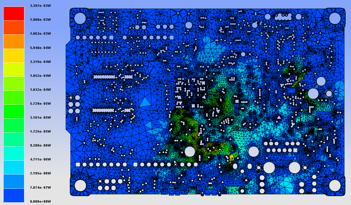
Figure 8 – Map of Power Loss in SIwave. This data is automatically transferred to IcePak.
ANSYS IcePak will not only give the user the temperature at every location on the board, components and in the air. It will also give insight on how the system functions.
“During the design process engineers can now understand immediately were the most critical temperatures are and how fast the flow in certain location is. Where does the flow form pockets and what overall effect does a fan has on my temperatures?”
Contour overlays can promptly answer all those engineering questions on how the PCB functions in its intended environment.
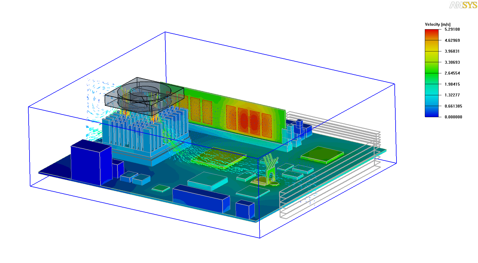
Figure 9 – Results: Temperature contours and fluid velocity vectors of a fan cooled rack mounted computer. Temperature contours give an overall performance indication of the cooling-management of the system. Velocity vectors of the flow add valuable insight and understanding of the heat flow mechanism and give constructive feedback for optimal design changes.
This example demonstrates the power of the ANSYS SIwave for efficiently simulating DC IR drop of PCB and also obtaining temperature rise together with the ANSYS Icepak. They provide an accurate calculation and visual elaboration on the DC voltage, current and power loss and temperature rise of PCB. It helps us to reach the design target by locating the hot spot of PCB and hence effectively optimising the PCB design
Thanks for reading! Hopefully you can now see the significant value in using ANSYS SIwave and Icepak to deliver a highly efficient solution for DCIR and thermal analysis of your PCB designs – to ensure a successful design for your next electronic product.