
The development of power electronics products always relies on transient circuit simulation to evaluate the internal operation of the product and the effect of outside conditions in a wide variety of scenarios. With this design style in mind, circuit simulation has developed to focus on being extremely fast and parametric to allow circuit designers to run hundreds and thousands of iterations on a design per day. However, as product performance reaches ever higher and the design limitations become ever tighter, circuit simulation is starting to lack the accuracy and functionality required to predict the more expensive design metrics.
Energy losses due to skin effects, nonlinearities due to saturable magnetics, trace/package coupling due to parasitics and high frequency harmonics due to fast switching semiconductors require detailed modelling to predict accurately. Modelling any one of these effects using lumped components is a challenging exercise in a lumped element circuit simulator, let alone attempting more than one. Certifying electronic products for Electromagnetic Compatibility (EMC) is quickly becoming one of the most costly parts of a product development, especially if multiple tests are required. Calculating and predicting the results of this test before the first prototype is built has the capacity to save significant test costs and accelerate time to market dramatically.
The ANSYS Electronics Desktop (AEDT) has been designed with this workflow in mind. In the early stages of design, thousands of design points can be run in a lumped element circuit simulator. As the development cycle progresses further, lumped components can be seamlessly exchanged for 3D geometry to continue the product optimisation with little in the way of performance loss. This allows designers to easily balance the time constraints imposed on the development cycle.
A Development Cycle Example – Electric Fence Energizer
An energizer is used to store a pre-defined amount of electrical energy and then discharge it in a safe manner onto a conductive. This allows fences which are not physically capable of restraining the animals in question to be built with adequate deterrence. At the same time while deterring animals, the fence must not be harmful to human beings who happen to be in contact momentarily.
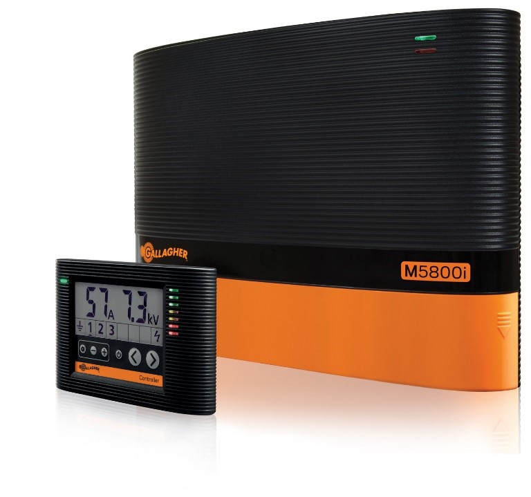
Figure 1 – Gallagher M5800i Energizer. Image courtesy of the Gallagher Group (https://gallagher.media/wp-content/uploads/2014/12/M5800i-Energizer-and-Controller.jpg)
Lumped Circuit Analysis
The general design consists of three main sections, a charging circuit to generate high voltage, a network of storage capacitors and a discharge circuit to generate high voltage pulses while safely isolating the fence from the mains supply.
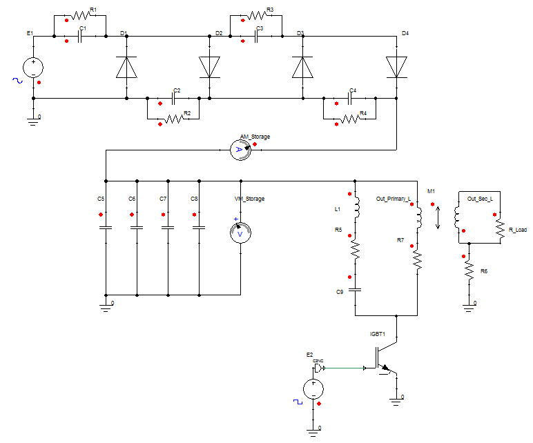
Figure 2 – Lumped Element circuit model of a simple energizer
This simulation assumes ideal components and no parasitics which is reasonable for general design iterations but very poor for detailed optimisation and verification. The following bullet points outline some typical design questions which could be evaluated and how long each would take to answer. All times were measured on a Dell Precision M6800 laptop using a single core:
- How many multiplier stages do I need to reach 1000V?
- Add an extra stage and solve (1 solve with a schematic change, 27 seconds)
- How fast does the charge circuit reach 800V? What is the peak current through the diodes?
- Sweep multiplier capacitor capacitance value (20 values, 2 minutes)
- What is the optimum ratio and values of inductance for the transformer primary/secondary windings in order to reach 7kV with a 500Ω load?
- Sweep primary/secondary inductance (90 values, 9 minutes)
- What output voltage and current is measured given a range of potential output loads?
- Sweep output load resistance (13 values, 1 minute 20 seconds)
For each of these simulations, all of the generated waveforms are available for review. As an example we could evaluate the stress imposed on the storage capacitors by measuring the voltage and current during a number of charge/discharge cycles.
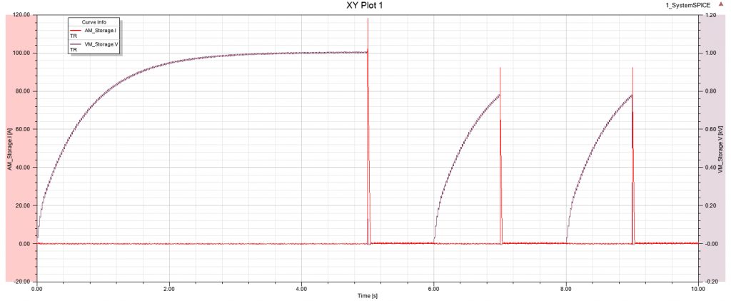
Figure 3 – Charge/Discharge cycle of the storage capacitor bank
Depending on the length of grass, condition of the fence and the weather, an electric fence an effective load resistance which varies dramatically. The AEDT can automatically produce a set of output waveforms with each design change to graphically represent how the energizers performance changes based on the load resistance and therefore track performance improvements over time. Architecture changes can be implemented easily at this stage so the EMI performance of the pulse is also evaluated to establish a base line.
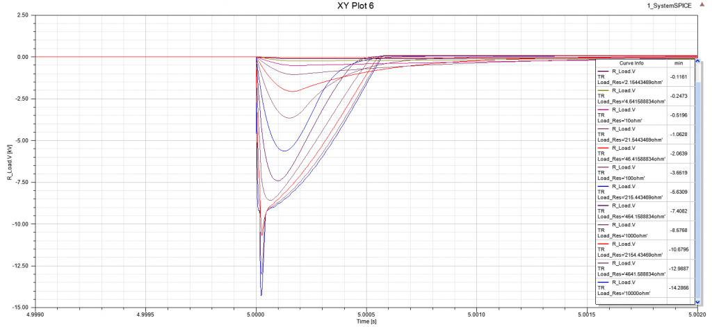
Figure 4 – Energizer output waveform for a range of output loads from 1Ω to 10000Ω
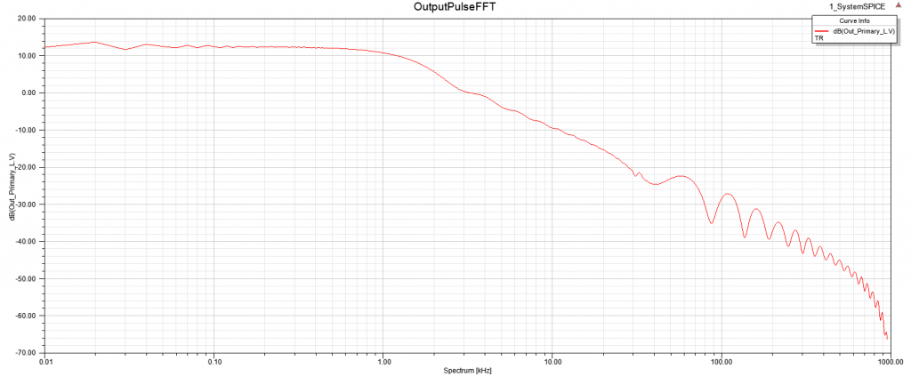
Figure 5 – FFT of the output pulse into a 500Ω load
Finite Element Analysis – Transformer Inductance and Capacitance
The energy generated at the output of the transformer needs to be limited to meet safety standards while still delivering high output voltages and currents when required to adequately drive the fence load. This depends on accurately designing the core to saturate under certain conditions and limit the output power. As with the circuit simulation, there are some key design questions that are evaluated at this stage:
- What dimensions should the core have for a given energy output?
- In 2D Magnetostatic, sweep through core sizes and current magnitudes to tune saturation levels (100 variations, 2 minutes)
- How many turns should each coil have to meet the required magnetic field intensity and circuit impedance?
- In 2D Magnetostatic, sweep through coil turns vs. coil current (10 variations, 1 minute)
- How does the coupling coefficient change with current amplitude for a given resistive load?
- In 2D transient, solve for a fixed input sinusoidal source (2 minutes per solve)
- How much capacitance exists between windings and the grounded core?
- In 2D Electrostatic, solve for the capacitance matrix (less than 1 second)
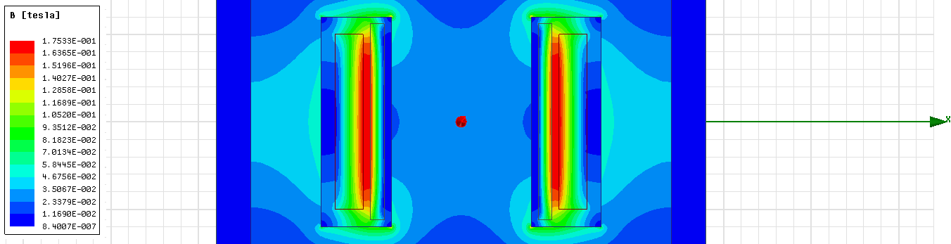
As part of the design process for the transformer, a characterised model can be generated that is valid for a wide range of current excitations and includes an accurate representation of the impact of core saturation. Finite element simulations include the capability to visualise the calculated fields either at steady state or during a transient run. Below is a plot of magnetic fields within an example design at a low current level.
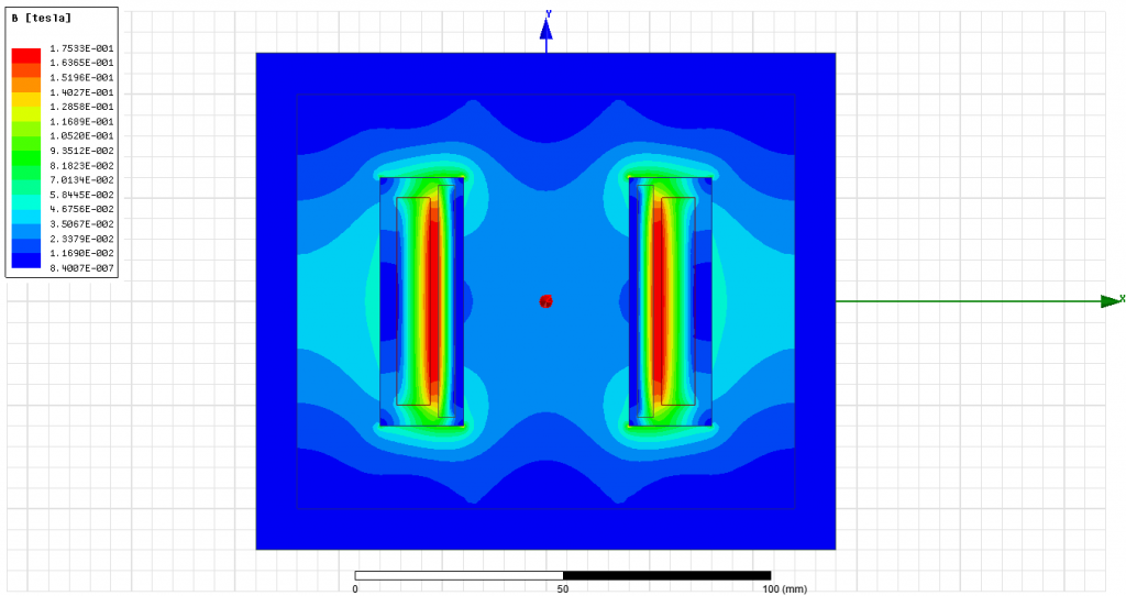
Figure 6 – Magnetic Field within the transformer core and around the winding
Semi-conductor Modelling
Obtaining accurate semiconductor models for use in circuit simulations is also a challenge. Very rarely are up to date component models available for all circuit simulators which invariably leads to assumptions being made about the devices performance under the conditions specified. Using the automated wizards within the AEDT, datasheets can be scanned and characterised to include all non-linear aspects of a devices performance including temperature variations. This provides a dramatic improvement in accuracy for power electronic circuits as well as convenience for the user.
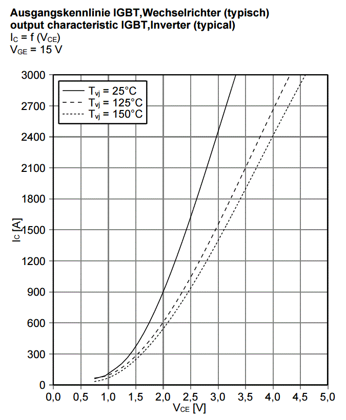
Figure 7 – Collector Current vs Collector-Emitter Voltage for an Infineon FZ1500R IGBT module
Circuit Simulation with Coupling
Taking the circuit simulation done in the previous step, it is simply a matter of replacing components with their more accurate representations and running the same workflow through again. Here is the new circuit with the nonlinear transformer magnetics, transformer capacitance matrix and characterised IGBT model.
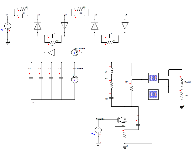
Figure 8 – Circuit simulation with characterised components
The same post-processing steps are retained from the previous simulation so it is simply a matter of running them again to produce the plot of output wave forms vs. effective load resistance. There is a significant change in the results when compared with the last steps. The overall voltage achieved by the design has dropped significantly and there are now new resonant components, the most severe of which occur at very high effective load resistance levels. Comparing the previous FFT results at 500Ω with the new waveform indicates that EMI is quickly becoming a problem for this design configuration.
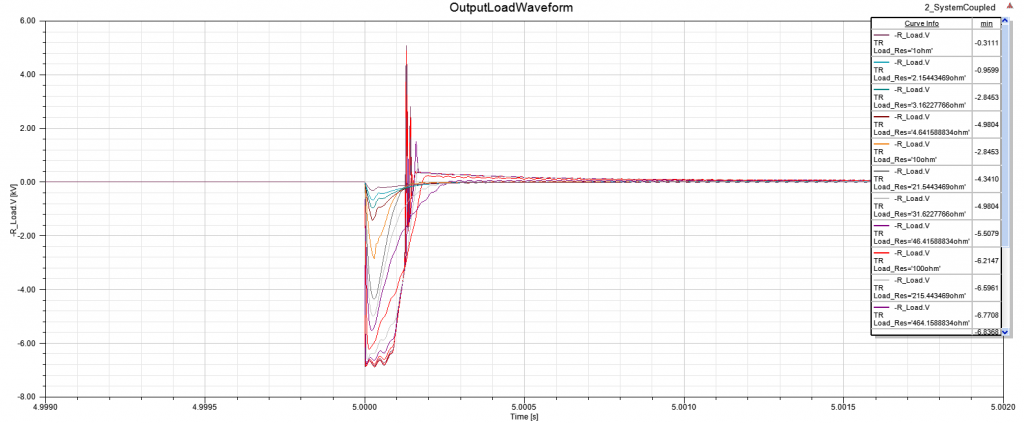
Figure 9 – Energizer output waveform for a range of output loads from 1Ω to 10000Ω including nonlinear components
Figure 10 – FFT of the output pulse into a 500Ω load. Comparison between original ideal component simulation (blue) and characterised components (red)
The overall energy in the pulse has dropped slightly but a significant amount of energy has shifted from the low frequency components into the higher frequencies. At this stage it would be prudent to re-balance the RFI components in the system to match the transformer but we will continue on for the sake of the example.
PCB Simulation
Up until now the losses due to the geometry connecting the components has been ignored but at high currents and frequencies, its behaviour becomes an important factor. The PCB geometry is characterised by measuring the s-parameters between each circuit connection point and then loading into the circuit simulator.
PCB designs often have a large number of competing factors which must be decided between.
- Maximising conductive area to reduce resistance and maximise output efficiency
- DC conduction simulation (20 seconds per solve)
- Minimising reflections at higher frequencies to avoid conductive or radiative EMI
- Power Integrity simulation from DC to 100MHz (1 minute per solve)
Below is a contour plot of the current densities in the discharge path just after the IGBT triggers.
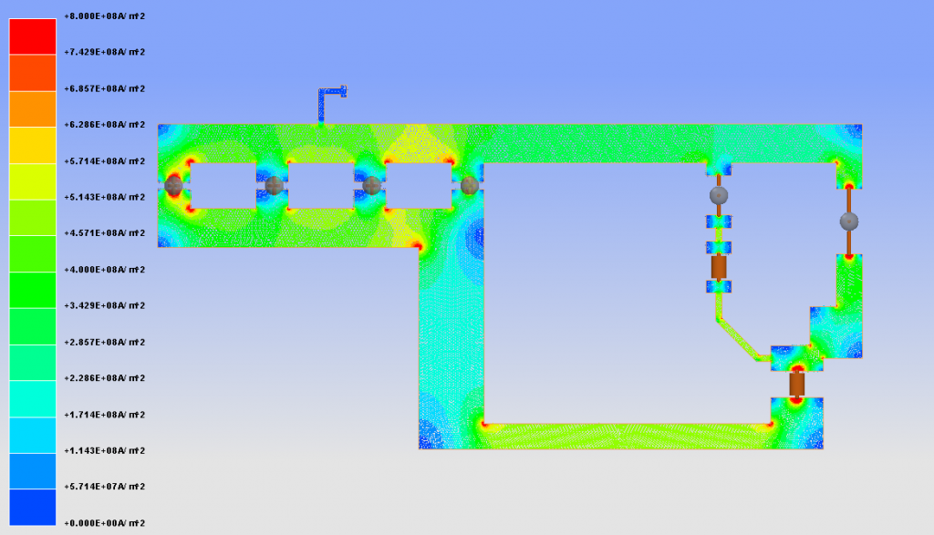
Figure 11 – Current densities in discharge path 50µs after the IGBT triggers
The energy losses in the discharge path have a significant effect on the output waveform and the distribution of frequency content in the waveform. The peak voltage achieved has dropped even further from 7kV down to just above 3kV. Now the design no longer achieves its performance targets and will need to be improved before going to production. The addition of new frequency dependent effects also changes the EMI performance of the output.
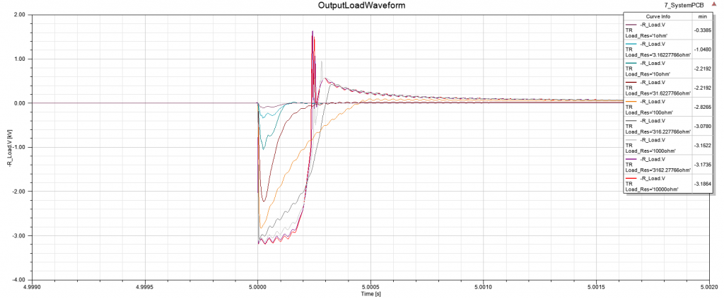
Figure 12 – Energizer output waveform for a range of output loads from 1Ω to 10000Ω including nonlinear components and the PCB
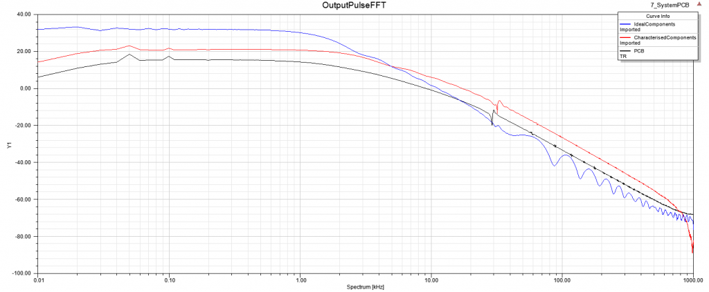
Figure 13 – FFT of the output pulse into a 500Ω load. Comparison between original ideal component simulation (blue), characterised components (red) and characterised components plus PCB (black)
Simulation Time versus Simulation Fidelity
The time taken to simulate an electronic product should always be significantly less than that taken to build and manufacture a prototype. It also comes with the advantage of simulating an ideal test environment and being easily repeatable. Table 1 outlines the time to simulate on a single core and the number of simulations which can be completed per day. With the AEDT HPC architecture, these numbers can be scaled to hundreds or thousands of parallel simulations to increase productivity even higher.
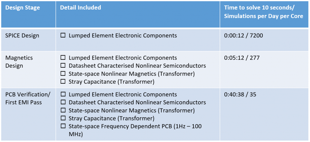
Table 1 – Comparison to complete 10 seconds of simulation time on a single core compared to the level of detail included
This workflow produces a design simulation which can be easily modified and has the capability to include even more advanced models such as certified ISO26262 software and thermal models to evaluate EMI performance with respect to warm up time.
In conclusion, the ANSYS Electronics Desktop provides a highly efficient solution for high fidelity electronics design and optimisation.
Jonathon McMullan
ANSYS Applications Engineer (Electromagnetics and Systems)